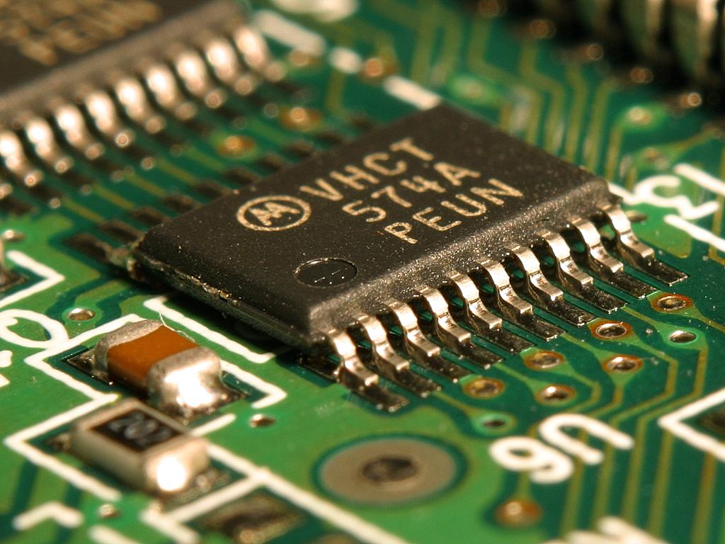
What happened: As chip design moves toward chiplet architectures, the physical assembly of separate dies onto a single interposer has become more complex than the underlying lithography. Major OSAT (Outsourced Semiconductor Assembly and Test) providers are currently reporting prolonged backlogs for advanced 2.5D and 3D packaging lines through late 2026.
Why it matters: Consumers and enterprise buyers frequently blame silicon wafer shortages for hardware delays, but current industry data points squarely to packaging capacity. Without sufficient packaging lines, even fully fabricated wafers sit idle, delaying product launches for servers and client devices alike.
Deep dive: Advanced packaging involves stacking memory alongside compute logic using microscopic copper pillars and silicon vias. Maintaining high yields across these dense interconnections requires extreme precision. When a single defect ruins a multi-billion-dollar assembly, manufacturing costs spike and overall throughput drops significantly, affecting equipment makers and end-users.
Report check (claims vs what is verified vs still rumor): Supply-chain analysts claim packaging capacity will double by Q4 2026. Verified reports confirm that key equipment suppliers face component lead times exceeding nine months. Rumors persist that major hyperscalers are securing exclusive multi-year packaging reservations, though independent audits have not verified these agreements.
Open questions: How quickly can independent foundries scale their internal packaging capabilities to rival specialized OSAT houses? Will emerging glass-substrate technologies alleviate these assembly constraints before 2027?